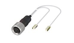
The BOH00EZ wafer mapping sensor uses a precise photoelectric sensor for quick and reliable detection of semiconductor wafers and slotting errors in front opening unified pods (FOUPs). Especially designed for use with extremely thin end effectors, it features a controlled and focused light spot, allowing it to detect wafers just a few μm thick. Based on photoelectric Micromote technology, it features a small LED sensor that measures 2.4 mm x 1.5 mm x 7 mm. This allows it to deliver precision even in small spaces.

